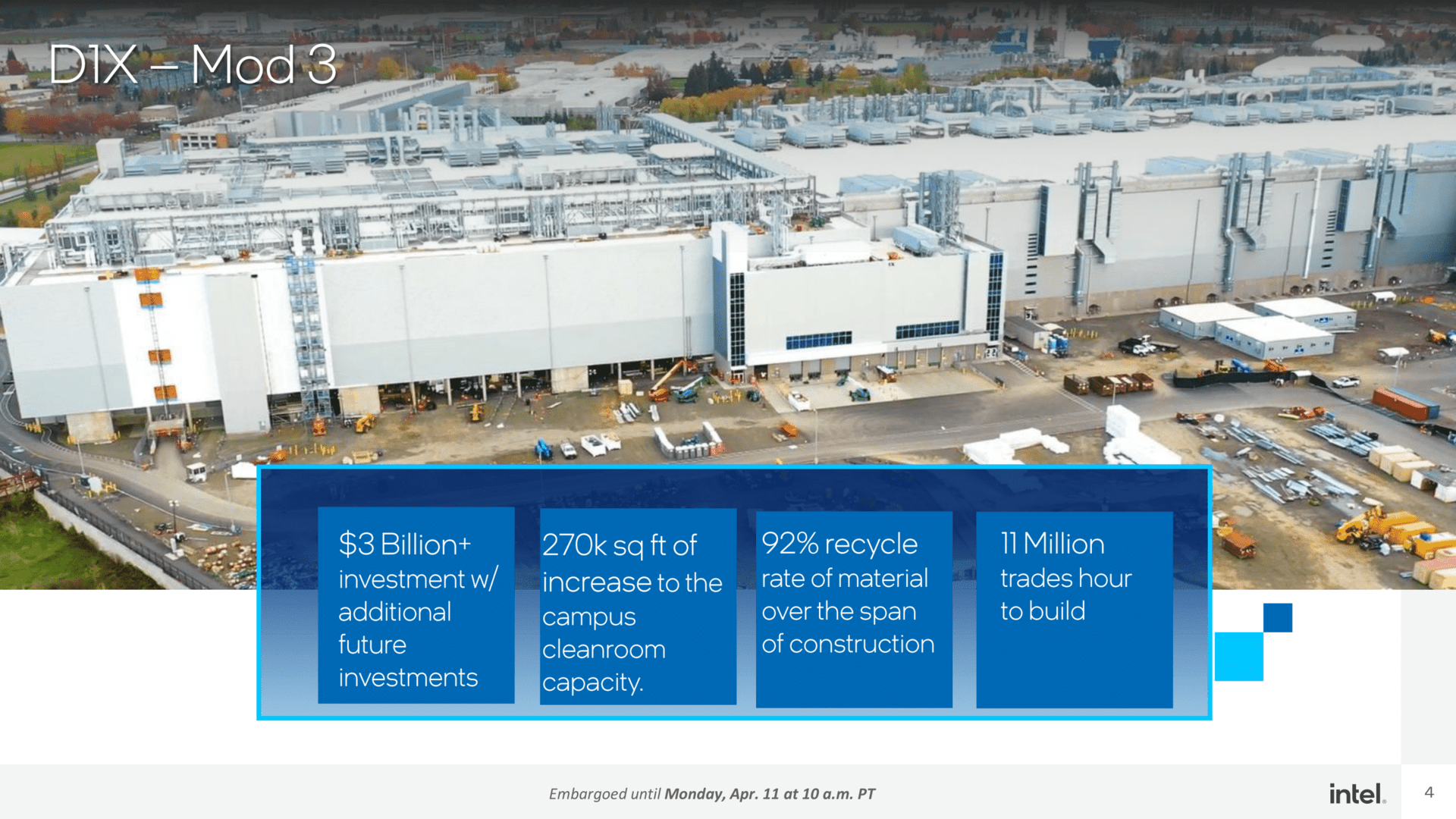
Intel’s research and development factory D1X has been expanded with a new module. Among other things, new EUVs with high NA are to be tested here. New machines need new buildings, so to speak, because they are bigger, heavier and, above all, higher. At the same time, Intel provided insight into further developments.
R&D back in focus
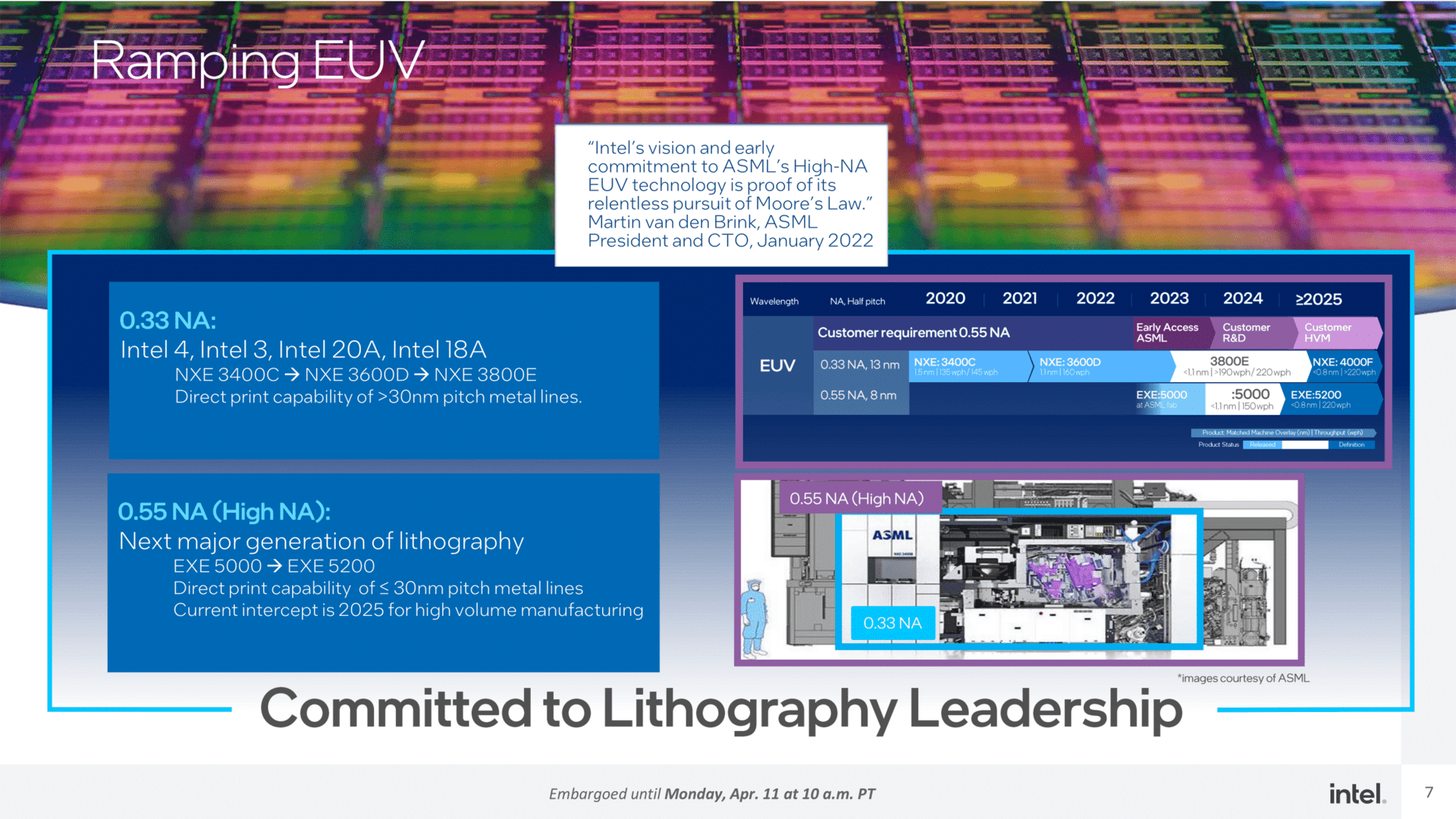
The $3 billion investment in a research and development factory is a staggering sum. The building’s clean room area, called the D1X, grows only a little over 20 percent, but the new area has it all: In the new module, not only the upcoming, classic EUV tools are to be used, but for EUVs with higher NAs. The foundation stone should be laid. The fact that this required new buildings should also be an issue for Intel’s factories around the world in the future.
So the new Mod3 of the D1X is probably also the blueprint that will be implemented in future factories. After all, Intel will be building several new plants over the next few years, and a campus in Magdeburg, Germany was also recently confirmed.
-

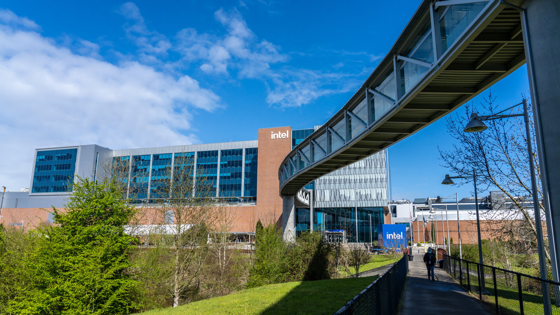
Intel Ronlar Acres with the new building on the left (Picture: Intel)
Picture 1 2 . from
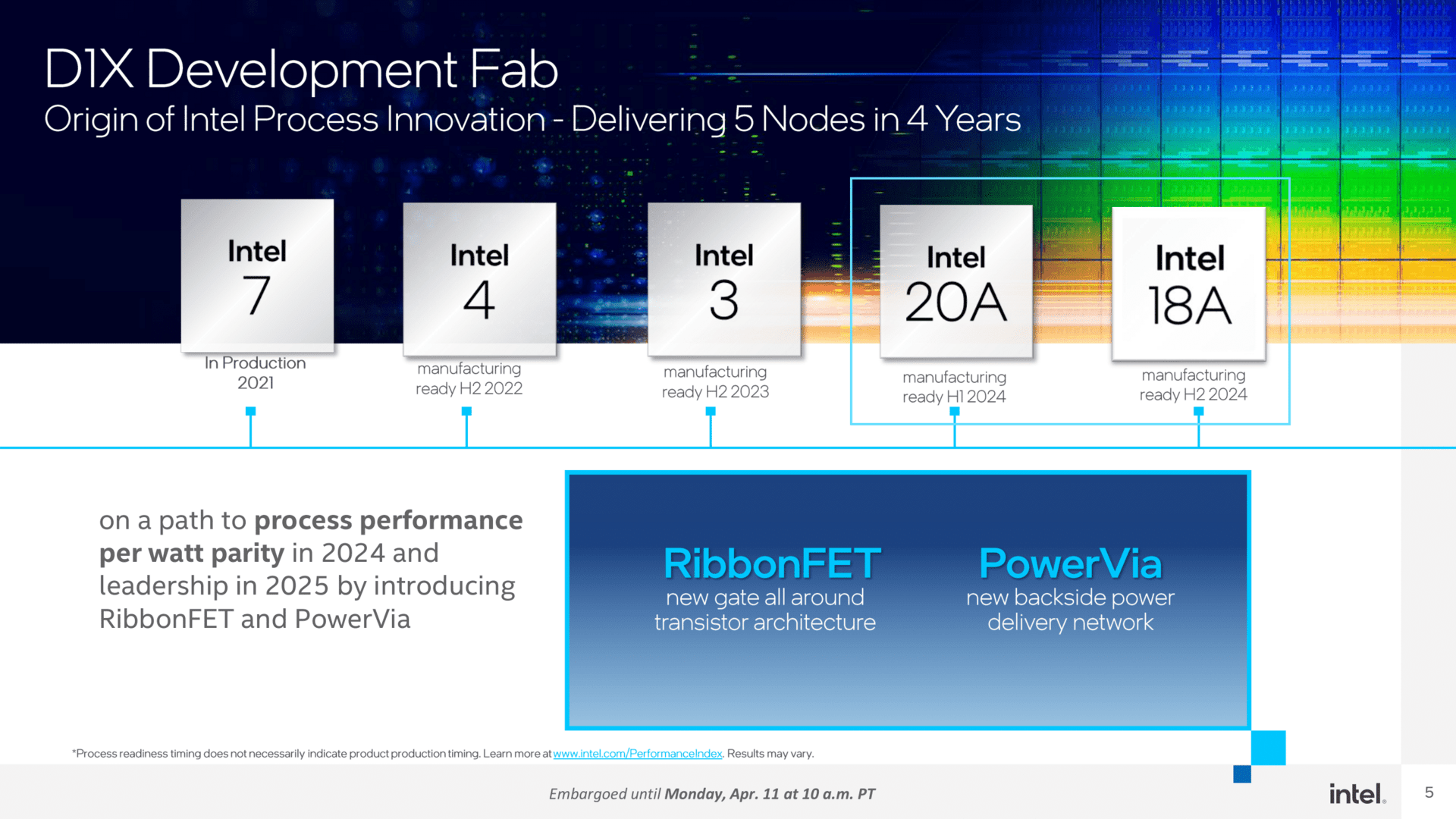
If things don’t work out as planned with the Hi-NA EUV, the factory will conduct further trials in the coming years. Preparing for failure and having a Plan B up its sleeve was not a feature of Intel of late. According to Intel, the backup plan that has already been taken into account, which should be able to implement production phases with classic EUV exposure, will be effective in the near future. The processors potentially affected are primarily the Intel 20A, but also the Intel 18A, which was recently pushed back a bit and should be ready for series production by 2025, just six months after the Intel 20A. Today Intel is said to be bridging the gap with classic EUV lithography by 2026.
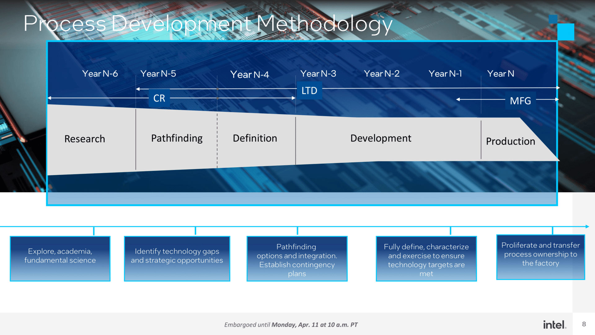
Intel states six years until a process matures from drawing board to series production. The Component Research (CR) department is in charge for the first few years, with the manufacturing group joining only later.
-
From research and development to product (Image: Intel)
Picture 1 3. Of
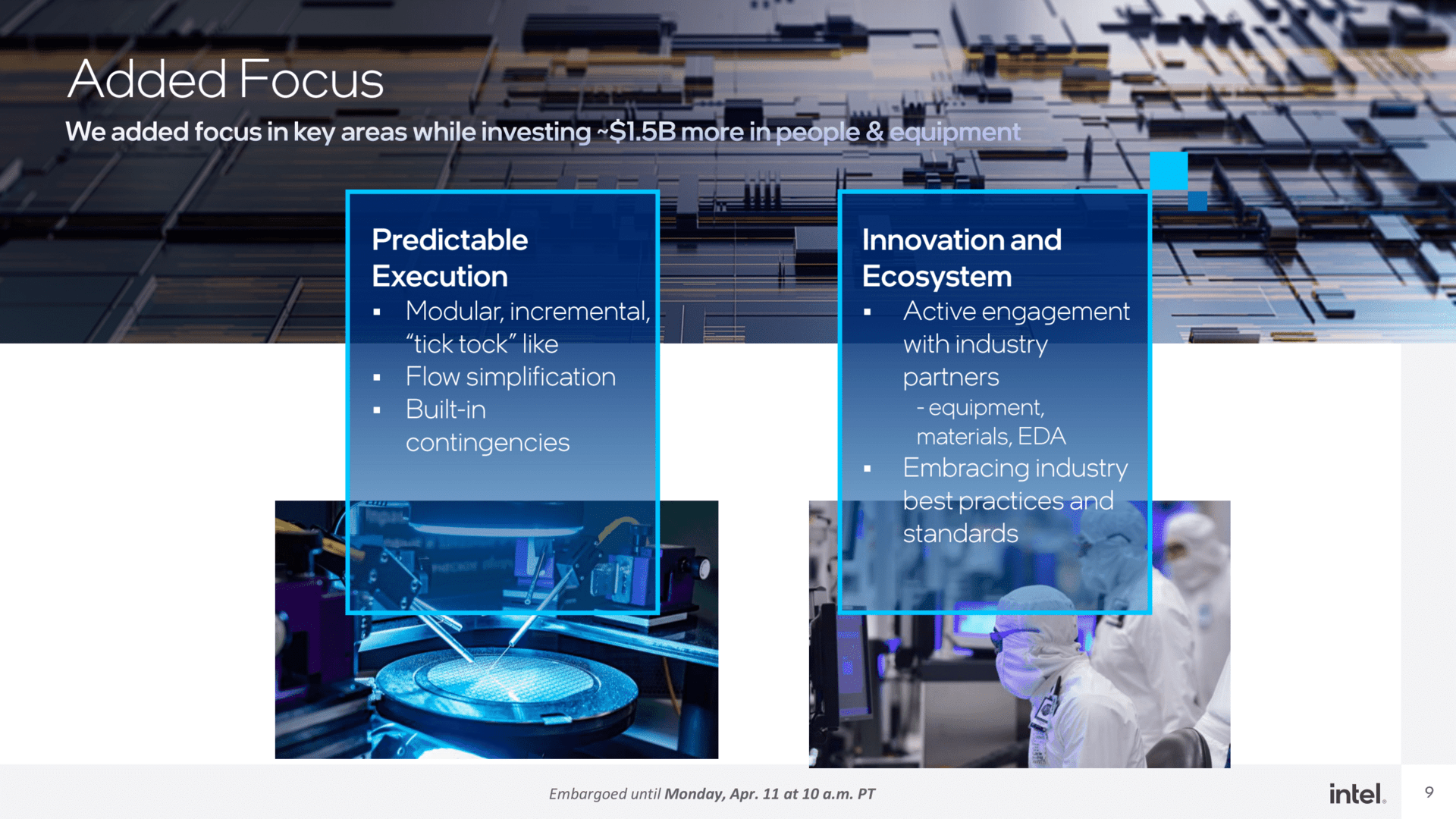
In the end, of course, it’s all a question of money. Here, Intel’s new CEO recently pulled out the checkbook and released more money to speed up implementation. However, collaboration with partners and the use of equipment used by other manufacturers deviates from the previous Lone Wolf approach. Much of what Intel is doing in factories is completely incompatible with other processes, and it starts with the design tools.
don’t repeat past mistakes
In statements made to the press last week, it became clear that Intel does not want to repeat the mistakes of the past, especially those that led to the 10nm nightmare. What the manufacturer is publicly presenting as an innovation for the future seems quite bizarre, because from the outside, such a mechanism should have been in effect in the past.
The fact that it didn’t exist, in retrospect, explains well why 10nm failed so badly on the first attempt and why it took Intel years to get back on track. In the end, the only thing that helped was to remove half the target for 10 nm and start from scratch. Intel has learned from this as well: The timeline of the technology roadmap doesn’t mention a year.
In the future, teams working on a process or technology for a new node should continue to work with this technology in the future. There are other teams that support and don’t have to leave as soon as something new is planned. And with completely new processes, Intel no longer wants to implement everything at once in the future – which ultimately broke 10nm’s neck on the first attempt.
And so Intel still has to build in the bug-fixed and optimized 10nm, although it is now marketed as Intel 7. After 7 years of planning, which once envisaged a very optimistic introduction of 10nm in 2015. Then what was it called By Intel in 2012: “We know how to make 10nm chips“. The next few years showed that was not the case.
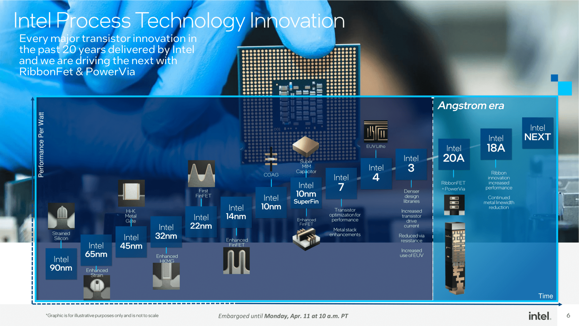
Internal intermediate process before PowerVia and GAA
This is best illustrated by the intermediate process that followed Intel 3. It is not intended to produce any products, but is handled internally as an independent node. Intel is testing the new PowerVia with the classic FinFET on it. With this approach, a large potential source of error other than PowerVia to test is nearly impossible. FinFETs have been around for over a decade, a proven technology. If problems do arise, they should be attributed to PowerVia. Intel hopes a solution can be found more quickly then.
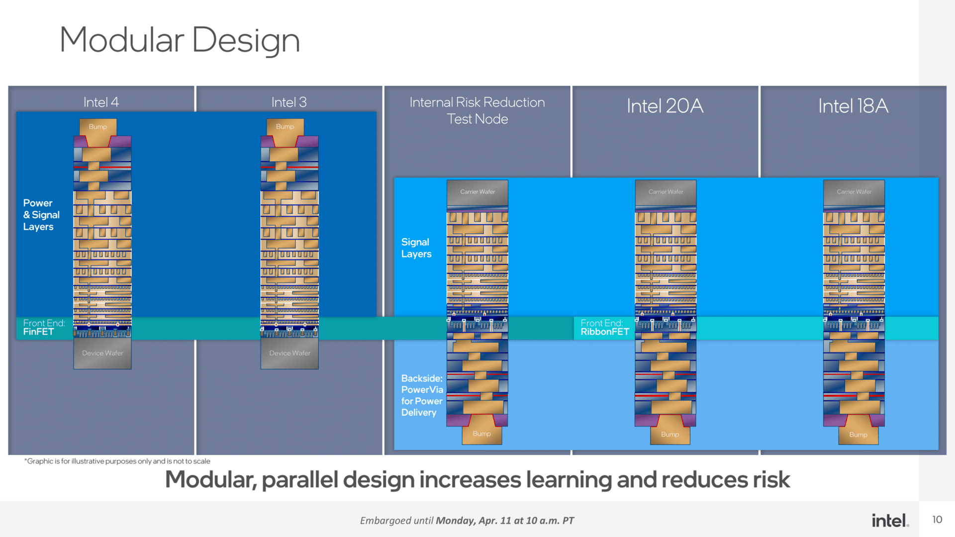
Once development is complete, a get-all-around (GAA, Intel calls this a RibbonFET) is introduced to the subsequent node. The first process thus implemented is the Intel 20A. But like many first of its kind, it will only be used in series for a short time according to current plans. Intel 18A should follow as a customized version within six months.
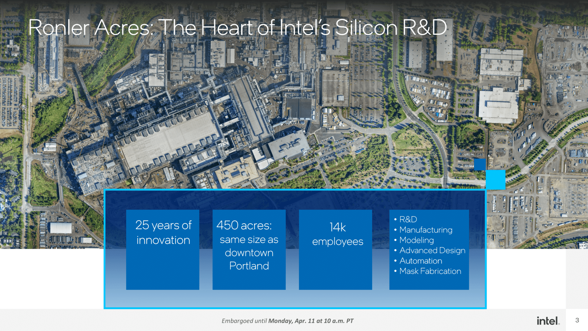
Ronler Acres becomes Gordon Moore Park
Intel properties in the US are often named after objects found on a piece of land. In Hillsboro, Oregon, for example, there is Hawthorne Farms and, even better, Jones Farms, in which not only are technologies developed, but loads of events are carried out – the computerbase has also at times been.
The Ronler Acres complex, with its factory buildings around D1C, D1D and D1X and the outbuildings used to follow this naming convention, but that is changing today. In tribute to Intel’s greatest and most famous personality, Gordon Moore, the entire campus is today Gordon Moore Park renamed at a ceremony,
Intel has a total of 22,000 employees at four locations in Hillsboro. According to its own statements, over US$52 billion has been invested in Oregon so far.
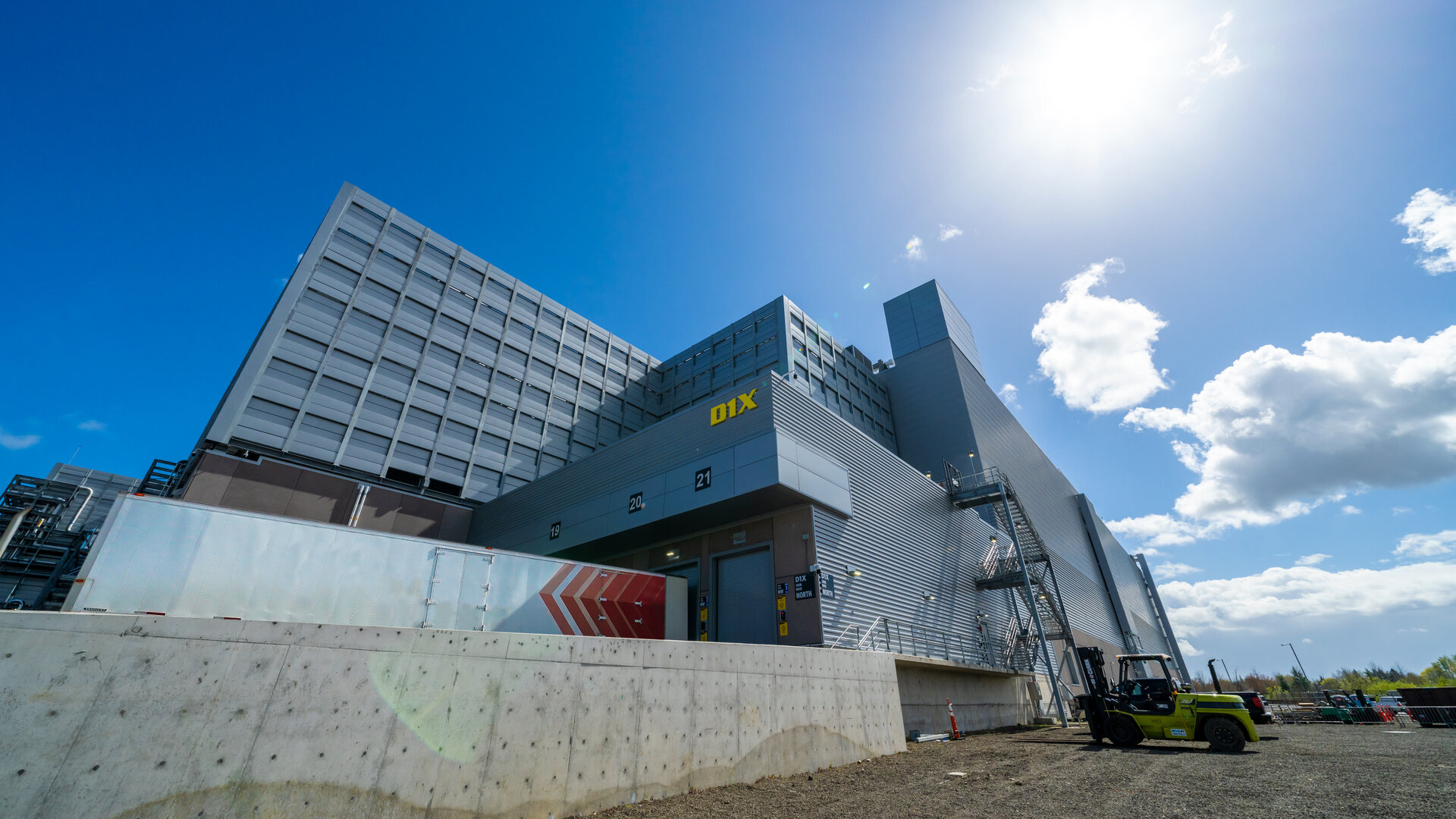
-
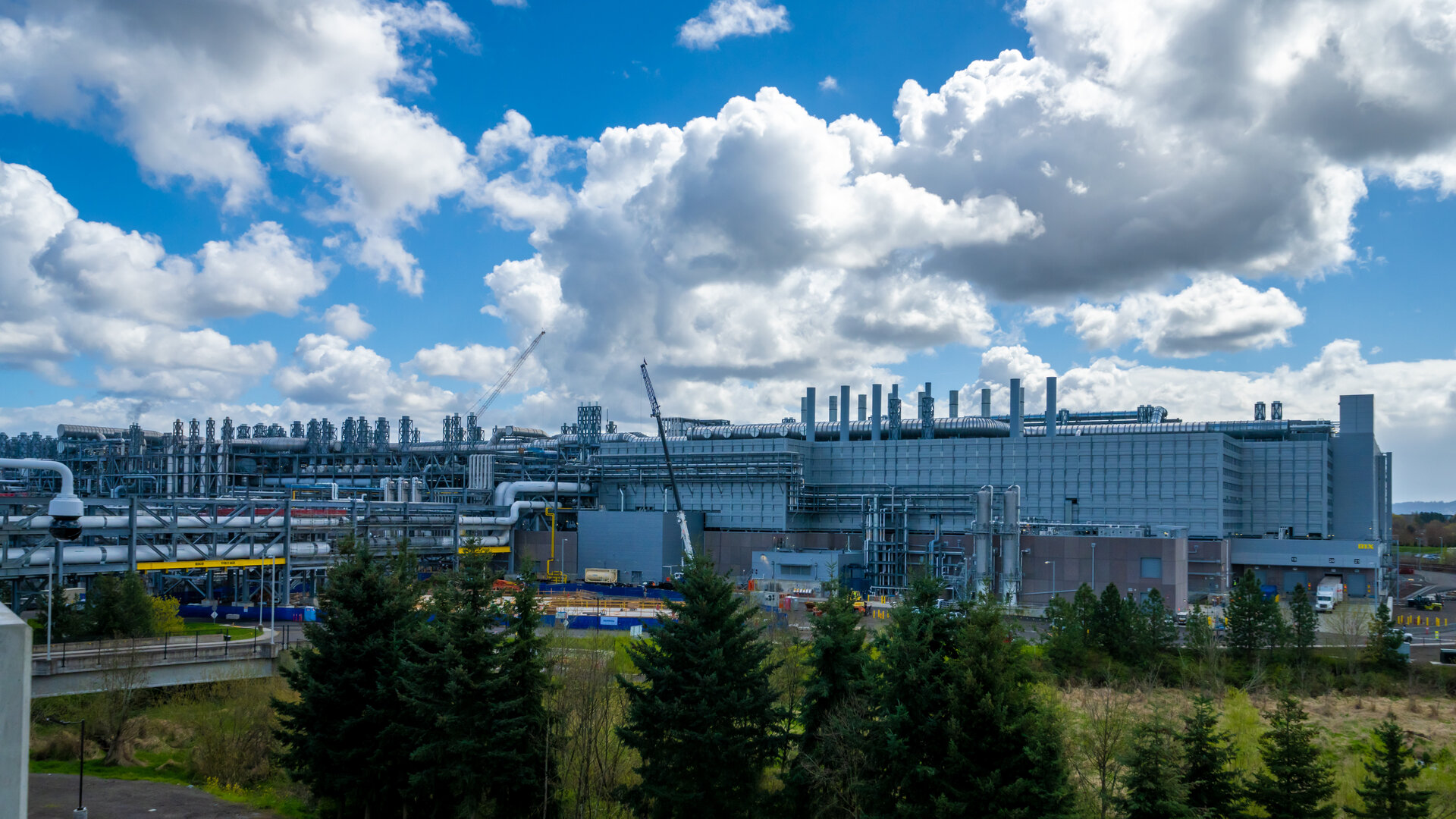
Intel D1X (Image: Intel)
Picture 1 3. Of
Computerbase received information about this article from Intel under an NDA. The only requirement was the earliest possible publication date.

Connor Beaumont is a contributor to CA News Ottawa, covering news, politics, business, technology, sport, entertainment, and lifestyle. He focuses on clear, accurate reporting and useful information that helps readers stay informed about current affairs and developments that shape their communities. His work highlights relevant stories, emerging trends, and important issues, presenting them in a balanced, accessible, and reader-friendly manner.